
CST STUDIO SUITE ELECTROMAGNETIC FIELD SIMULATION SOFTWARE
CST STUDIO SUITEELECTROMAGNETIC FIELD SIMULATION SOFTWARE
Electromagnetic Field Simulation Software
CST Studio Suite® is a high-performance 3D EM analysis software package for designing, analyzing and optimizing electromagnetic (EM) components and systems.
Electromagnetic field solvers for applications across the EM spectrum are contained within a single user interface in CST Studio Suite. The solvers can be coupled to perform hybrid simulations, giving engineers the flexibility to analyze whole systems made up of multiple components in an efficient and straightforward way. Co-design with other SIMULIA products allows EM simulation to be integrated into the design flow and drives the development process from the earliest stages.
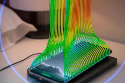
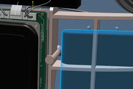
Common subjects of EM analysis include the performance and efficiency of antennas and filters, electromagnetic compatibility and interference (EMC/EMI), exposure of the human body to EM fields, electro-mechanical effects in motors and generators, and thermal effects in high-power devices.
CST Studio Suite is used in leading technology and engineering companies around the world. It offers considerable product to market advantages, facilitating shorter development cycles and reduced costs. Simulation enables the use of virtual prototyping. Device performance can be optimized, potential compliance issues identified and mitigated early in the design process, the number of physical prototypes required can be reduced, and the risk of test failures and recalls minimized.
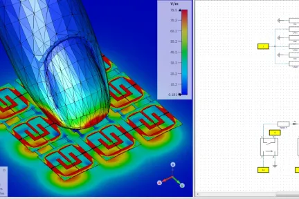
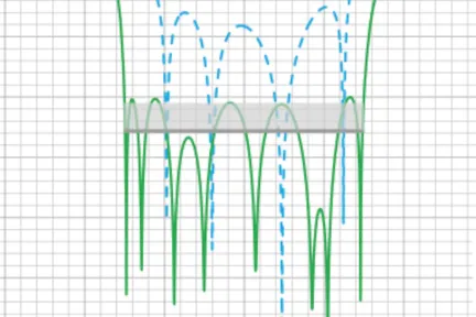
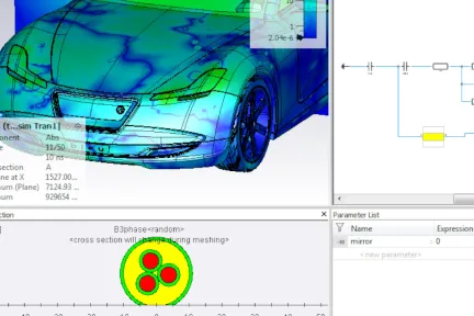
CST Studio Suite Simulation Solvers for Electromagnetic Systems and Devices
CST Studio Suite Offers Graphical User Interface for Electromagnetic Systems and Devices
CST Studio Suite Offers Automatic Optimization Routines for Electromagnetic Systems and Devices
CST Studio Suite Provides an Environment that Simplifies the Management of Simulation Projects
CST Studio Suite Import and Data Exchange Options to Streamline Electromagnetic Design
The world of Design & Simulation is changing. Discover how to stay a step ahead with SIMULIA.
CST STUDIO SUITEELECTROMAGNETIC FIELD SIMULATION SOFTWARE
CST Studio Suite is a commercial program that is available through the Dassault Systèmes channels. However, there is a free version: The CST Studio Suite Learning Edition introduces you to electromagnetic simulation, simplifying the comprehension of Maxwell’s equations. This free edition grants you access to our robust visualization engine and advanced solvers of CST Studio Suite, with a few limitations. It is perfect for coursework and individuals aiming to enhance their proficiency with CST software.
CST Microwave Studio (CST MWS) was the first product of the CST Studio line of software. Initially focussed on the finite integration technique (FIT) transient solver, it was well-suited for antenna and wideband applications. It also included FIT-based Eigenmode and frequency domain solvers. Later finite element method (FEM) and integral equation solvers followed. Finally, in 2006, CST Microwave Studio and the other CST software were integrated into the CST Studio Suite.
CST Studio Suite Software offers many advantages to the User. First of all, there is the intuitive user interface that simplifies typical modeling, post-processing and optimization tasks. Most importantly, there is the set of solvers, that efficiently deals with simulation across the entire electromagnetic spectrum, from statics to light. With the integration of CST simulation software in the 3DEXPERIENCE platform new benefits or CST Studio Suite users unfold.
CST is the acronym for Computer Simulation Technology. CST was the company that developed and marketed CST Studio Suite. It was acquired by Dassault Systèmes in 2016.
CST software is used for the simulation of electromagnetic fields across the entire electromagnetic spectrum. It allows engineers to experiment with virtual prototypes even at the earliest stages of the design process, to compare the performance of different configurations, and to optimize their products. Simulation can reduce the number of physical prototypes required and shorten the development process, cutting both costs and time-to-market. Products can be simulated as part of a realistic system to analyze their installed performance and verify they meet legal electromagnetic compatibility (EMC) and exposure limits, potentially avoiding time-consuming redesigns or costly recalls.
The CST Studio Suite Learning Edition is a software that helps you learn about electromagnetic simulation and simplifies the understanding of Maxwell's equations. This edition is free and provides access to the visualization engine and advanced solvers of the CST Studio Suite, with some limitations. It is ideal for students and individuals who want to improve their skills with CST software.
Electromagnetic (EM) simulations fall under the category of high-performance computing tasks. Therefore, computers utilized for CST applications need to meet stringent criteria concerning CPU, RAM, and graphical specifications to attain peak performance. Up-to-date information can be found in our CST Studio Suite support area.
Engineering Software from SIMULIA
Simulation and Analysis of Electromagnetic Fields
Speak with a SIMULIA expert to learn how our solutions enable seamless collaboration and sustainable innovation at organizations of every size.
Courses and classes are available for students, academia, professionals and companies. Find the right SIMULIA training for you.
Find information on software & hardware certification, software downloads, user documentation, support contact and services offering